Inside the Chiplet Revolution: How Arm CSS and CSA Democratize Custom AI Silicon

As artificial intelligence (AI) workloads surge in complexity and scale, the traditional system-on-chip (SoC) model is encountering a trifecta of challenges: power inefficiency, performance bottlenecks, and lengthening time‑to‑market. Chiplets address these pressures by letting teams reuse validated building blocks and scale only the dies that matter for a target AI workload. Monolithic chip design – once the domain of hyperscalers – can no longer keep pace with the demands of modern AI infrastructure.
At the 2025 OCP Global Summit, Arm is spotlighting a shift: chiplet‑based innovation, powered by Arm Compute Subsystems (CSS) and Chiplet System Architecture (CSA), now opening doors for silicon providers to build AI-optimized designs without needing the scale of a hyperscaler.
What’s the Difference Between Monolithic SoCs and Chiplet-based AI Silicon?
For years, full custom SoCs dominated the high end of AI infrastructure; everything from compute blocks to memory controllers, interconnects, and accelerators was integrated on a single monolithic die. While this design offered tight control and performance advantages, it also carried steep trade‑offs:
- Rising power and thermal costs as process nodes push limits;
- Complexity in validation and verification of large, heterogeneous blocks; and
- Long lead times for design, tooling, and manufacturing.
Enter chiplet‑based compute. By decomposing a system into smaller, specialized dies – compute, memory, I/O, accelerators, SoC architects and designers gain the ability to mix and match components, scale only what’s needed, and iterate faster. Until now, that modularity came with its own barriers: design fragmentation, lack of standardized interconnects, IP reuse challenges, and substantial upfront risk and cost.
How do Arm CSS and CSA Reduce Chiplet Fragmentation and Design Risk?
Arm is closing those gaps via two foundational frameworks:
- CSS: These are pre‑validated, high‑performance IP building blocks – compute cores, AI accelerators, memory subsystems – with design, verification, and performance profiles already proven in real or emulated silicon. Using CSS means designers don’t have to invent every block from scratch or re‑validate what works; instead, they leverage established, optimized pieces. Think of CSS as the ‘already-tested’ foundation that shortens verification cycles so teams can focus differentiation on accelerators, memory, and system integration.
- CSA: An open, standards‑driven architecture for how chiplets interconnect, communicate, and integrate across vendors. CSA defines electrical, physical, and protocol‑level compatibility so that IP from different sources – for example, accelerators from partner A, and memory dies from foundry B – can interoperate reliably on a shared platform. CSA’s goal is to reduce fragmentation by aligning system partitioning choices and chiplet connectivity so multi-vendor dies can integrate more predictably.
Together, CSS and CSA enable silicon providers – companies such as Socionext, Rebellions, and others – to build custom, AI‑optimized chips that deliver performance comparable to hyperscaler designs, yet with lower risk, faster cycle times, and more flexibility. These providers can pick and choose compute blocks, accelerators, memory types, and integration paths according to specific workload needs, like vision models, inference engines, and multi‑tenant instances, rather than being locked into monolithic design trade‑offs.
Why is OCP Important for Open Chiplet Standards and Interoperability?
The Open Compute Project (OCP) has long been a locus for open hardware collaboration, modularity, and efficiency – principles that align closely with the chiplet revolution. At the 2025 OCP Global Summit, Arm is demonstrating not just theoretical architectures but working examples of how CSS and CSA combinations are being used by cloud service providers (CSPs), OEMs, and silicon vendors to future‑proof their AI infrastructure.
Key benefits that OCP partners are seeing include:
- The flexibility to customize silicon for region‑specific power, thermal, or reliability constraints.
- Lower total cost of ownership (TCO) through supply chain optionality, which is the ability to source chiplets or dies from multiple foundries, mix and match dies as volumes scale, rather than being tied to a single monolithic vendor.
- Faster time‑to‑market, since validated CSS blocks and standardized interconnect allow much of the design work to be “already done,” enabling more rapid prototyping, testing, and deployment.
Business Impact and What Comes Next
For AI infrastructure builders – whether CSPs, OEMs, or silicon firms just stepping into AI work – the CSS and CSA approach offers real outcomes:
- Performance-per-watt improvements: Compute and memory are placed where they can be most efficient, without waste.
- Reduced design risk: By re‑using proven IP and relying on standard interconnects.
- Supply chain resilience: Modularity makes it more feasible to switch sources, scale die production, or choose preferred foundry nodes.”
- Speed: Design cycles shrink, allowing for faster iteration on AI models, feature sets, and deployment.
This is more than silicon architecture; it’s a business lever for agility in the age of AI.
Where Can You See CSS and CSA in Action?
At the 2025 OCP Global Summit, Arm will host sessions and technical briefings showcasing CSS and CSA in action. Whether you’re a silicon designer, infrastructure architect, or cloud provider exploring the future of AI hardware, this is your opportunity to see what’s possible beyond today’s constraints.
For a deeper dive into the tools and workflows enabling this shift, explore how developers are using the Arm Neoverse CSS V3 platform to accelerate pre-silicon validation and firmware development:
- Develop and Validate Firmware Pre-Silicon on Arm Neoverse CSS V3
- Simulate OpenBMC and UEFI Pre-Silicon on Neoverse RD-V3
These resources show how early software bring-up, firmware validation, and system prototyping are already happening, before silicon ever hits the fab.
Arm’s mission is clear: to make custom AI silicon accessible to all, not just the hyperscalers, because the future of the datacenter depends on innovation at every scale.
Any re-use permitted for informational and non-commercial or personal use only.
Editorial Contact


Latest on X
Agentic AI requires a new approach to infrastructure.
At #COMPUTEX2026, @Rebellions_inc showcased RebelCard™ and discussed how Arm AGI CPU and AI accelerators can work together to deliver scalable, energy-efficient AI inference.
Hear from Co-founder & CTO Jinwook Oh ⬇️

"We have almost a control tower view of the entire industry. We see everything. We talk to everyone."
On @TBPN, Arm CEO Rene Haas shared how our position at the center of the world's compute ecosystem gives us a unique perspective on the technology and trends shaping the next

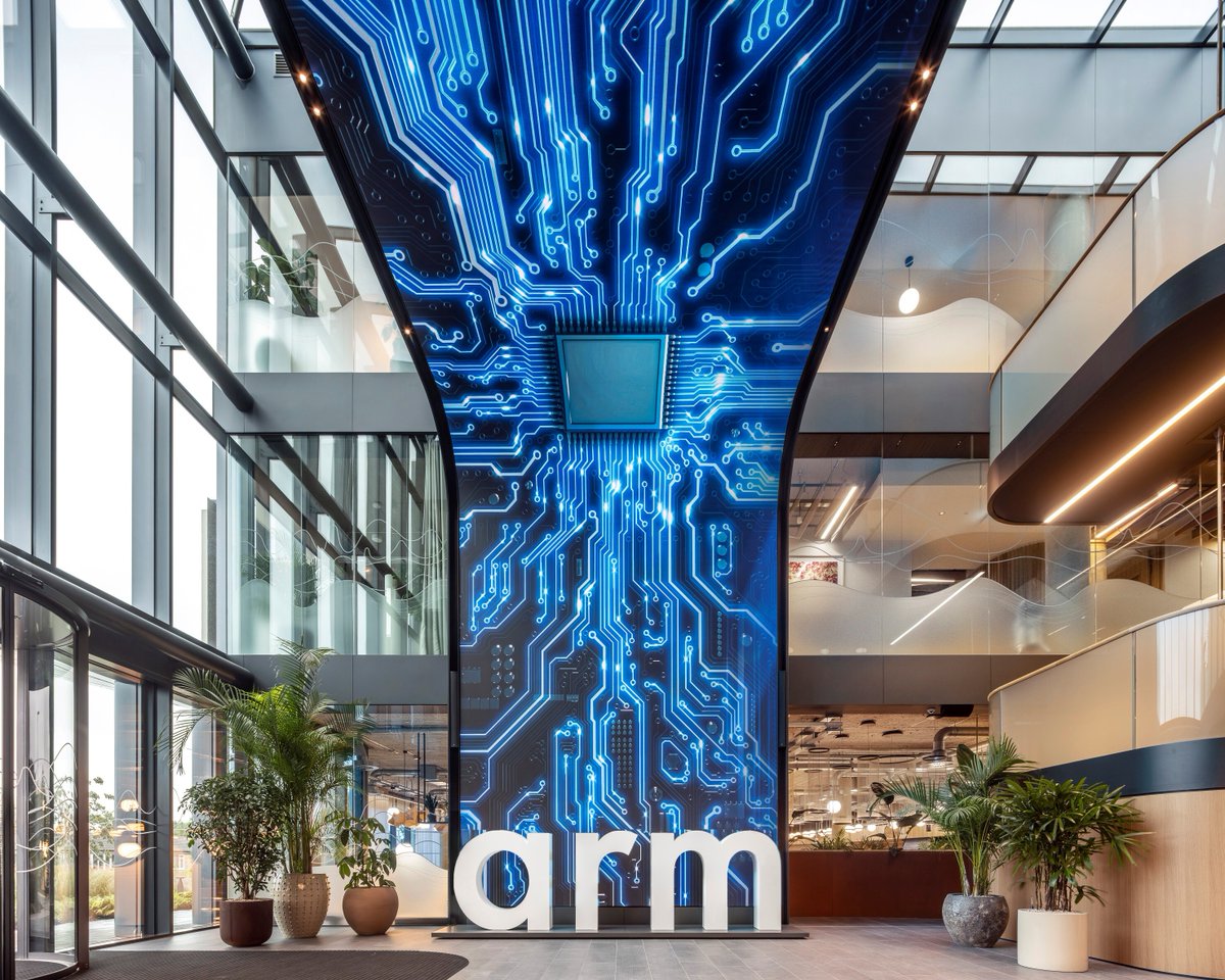
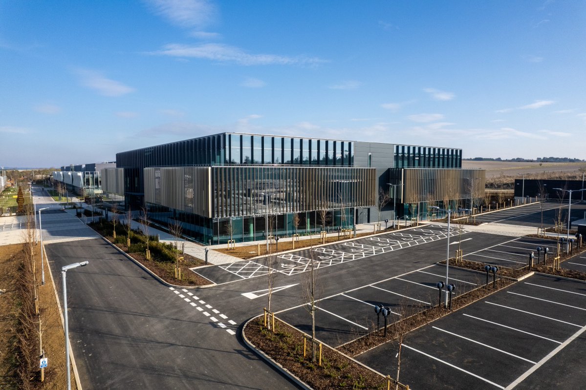
A new addition to Arm Cambridge. 🏢
We recently opened doors to E&F, the sixth building on our Cambridge campus, designed to support collaboration, innovation and growth for years to come.
Here's a look inside 📸


The future of AI infrastructure will be built as a system.
As AI workloads become more complex, performance alone isn't enough. Infrastructure must also be efficient, scalable and designed to work seamlessly across the stack.
At #COMPUTEX2026 @Rebellions_inc Co-founder & CTO

Today Arm hosted the Women in @TechworksHub: Engineering Intelligently event, bringing together innovators from across the technology industry to discuss leadership, transformation, and the future of talent in the AI era.
Alongside insights from Arm's Chief People Officer,


Congratulations to @Uber, @Nuro and @LucidMotors on announcing plans to bring robotaxi service to Houston in 2027.
Arm technology helps power the stack, from Nuro Driver on @nvidia DRIVE AGX Thor with Arm Neoverse V3AE CPUs, to Lucid Gravity's autonomous compute platform, to
At #COMPUTEX2026, @Lenovo showcased the Arm AGI CPU-based HR650a V3 Server.
Hear from John Donovan on why Arm was a natural fit and how the collaboration is helping deliver something different for AI and cloud infrastructure. https://okt.to/z8NG2S