Arm and TSMC Demonstrate Industry’s First 7nm Arm-based CoWoS® Chiplets for High-Performance Computing

Hsinchu, Taiwan R.O.C., September 26, 2019 – Arm and TSMC, the High-Performance Computing (HPC) industry leaders, today announced an industry-first 7nm silicon-proven chiplet system based on multiple Arm® cores and leveraging TSMC’s Chip-on-Wafer-on-Substrate (CoWoS®) advanced packaging solution. This single proof-of-concept chiplet system successfully demonstrates the key technologies for building an HPC System-On-Chip (SoC) with Arm-based cores operating at 4GHz in a 7nm FinFET process. The chiplet system also demonstrates for SoC designers an on-die, bi-directional interconnect mesh bus operating at 4GHz, and a chiplet design methodology connected by an 8GB/s inter-chiplet interconnect over a TSMC CoWoS interposer.
Rather than the traditional SoC approach of combining every system component onto a single die, chiplet designs are optimized for modern HPC processors which partition large multi-core designs into smaller chipsets. This efficient approach enables functions to be split into smaller, separate dies which provide for the flexibility of producing each chiplet on different process technologies, as well as delivering better yields and overall cost effectiveness. And to ensure the highest levels of performance, chiplets must communicate with each other through dense, high-speed, high-bandwidth connections. To address this challenge, this chiplet system features a unique Low-voltage-IN-Package-INterCONnect (LIPINCONTM) developed by TSMC which has reached data rates of 8Gb/s per pin with excellent power efficiency results.
Chiplet System Details
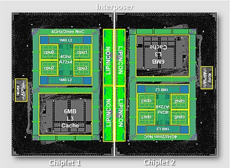
The chiplet system is comprised of a dual-chiplet CoWoS implemented in 7nm, with each chiplet containing four Arm Cortex®-A72 processors and an on-die interconnect mesh bus. The die-to-die inter-chiplet connection features scalable 0.56pJ/bit (pico-Joules per bit) power efficiency, 1.6Tb/s/mm2 (terabits per second per square millimeter) bandwidth density, and 0.3V LIPINCON low-voltage interface achieving 8GT/s (Giga Transactions per second) and 320GB/s bandwidth. The chiplet system was taped out in December 2018, and produced in April 2019.
“This latest proof-of-concept with our longtime partner TSMC is an excellent foundation for future production-ready infrastructure SoC solutions which will integrate TSMC’s innovative advanced packaging technology with the unmatched flexibility and scalability of the Arm architecture,” said Drew Henry, Senior Vice President and General Manager of Arm’s Infrastructure Line of Business
“This demonstration chip is an excellent showcase of the system integration capabilities we offer to our customers,” said Dr. Cliff Hou, Vice President of Technology Development for TSMC. “TSMC’s CoWoS advanced packaging technology and LIPINCON inter-chiplet interface enable customers to partition large multi-core designs into smaller chiplets that deliver better yield and better economics. This Arm and TSMC collaboration further unleashes our customers’ innovations in high-performance SoC design for cloud-to-edge infrastructure applications.”

Fig. 1: Dual Chiplet Floorplan
About Arm
Arm technology is at the heart of a computing and connectivity revolution that is transforming the way people live and businesses operate. Our advanced, energy-efficient processor designs have enabled intelligent computing in more than 150 billion chips. More than 70% of the world’s population are using Arm technology, which is securely powering products from the sensor to the smartphone to the supercomputer. This technology combined with our IoT software and end-to-end connectivity, device and data management platform enables customers to derive real business value from their connected devices and data. Together with our 1,000+ technology partners we are at the forefront of designing, securing and managing all areas of compute from the chip to the cloud.
About TSMC
TSMC pioneered the pure-play foundry business model when it was founded in 1987, and has been the world’s largest dedicated semiconductor foundry ever since. The company supports a thriving ecosystem of global customers and partners with the industry’s leading process technology and portfolio of design enablement solutions to unleash innovation for the global semiconductor industry.
TSMC serves its customers with global capacity of more than 12 million 12-inch equivalent wafers per year in 2019, and provides the broadest range of technologies from 0.5 micron plus all the way to foundry’s most advanced processes, which is 7-nanometer today. TSMC is the first foundry to provide 7-nanometer production capabilities, and is headquartered in Hsinchu, Taiwan.
# # #
TSMC Spokesperson:
Wendell Huang
Vice President and CFO
Tel: 886-3-566-5920
TSMC Acting Spokesperson:
Elizabeth Sun
Senior Director
Corporate Communications
Tel: 886-3-568-2085
E-Mail: elizabeth_sun@tsmc.com
For Further Information:
Michael Kramer
Project Manager
PR Department
Tel: 886-3-5636688
Ext. 7125031
Mobile: 886-988-931-352
E-Mail: pdkramer@tsmc.com
Any re-use permitted for informational and non-commercial or personal use only.


